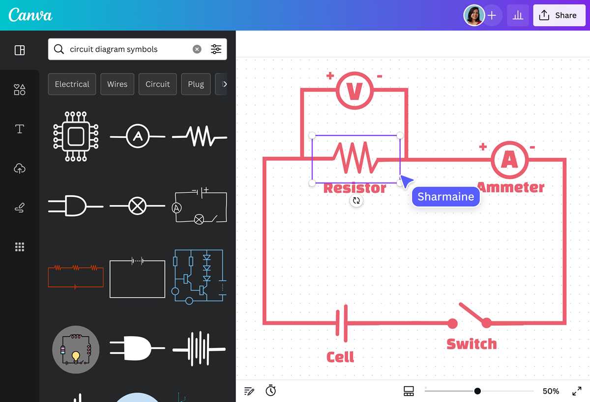
Prioritize a clear schematic of each component and their connections. Identify resistors, capacitors, transistors, and integrated modules, then assign their terminals and polarity before arranging them on a visual grid. Use consistent labels to avoid confusion during assembly.
Verify signal flows and voltage paths between nodes. Trace each path from power sources to endpoints, marking junctions and potential overlaps. Highlight critical lines carrying high current or sensitive signals to prevent interference.
Use color coding and line styles to separate functions. Distinguish data lines, control paths, and grounding tracks with distinct colors or dashed lines. This approach minimizes misrouting and simplifies troubleshooting.
Simulate the layout on software before physical assembly. Test virtual connections for shorts, voltage drops, and component compatibility. Adjust spacing and orientation to reduce noise and maintain accessibility for adjustments or replacements.
Step by Step Guide to Creating Accurate Electronics Layouts with Labeled Connections
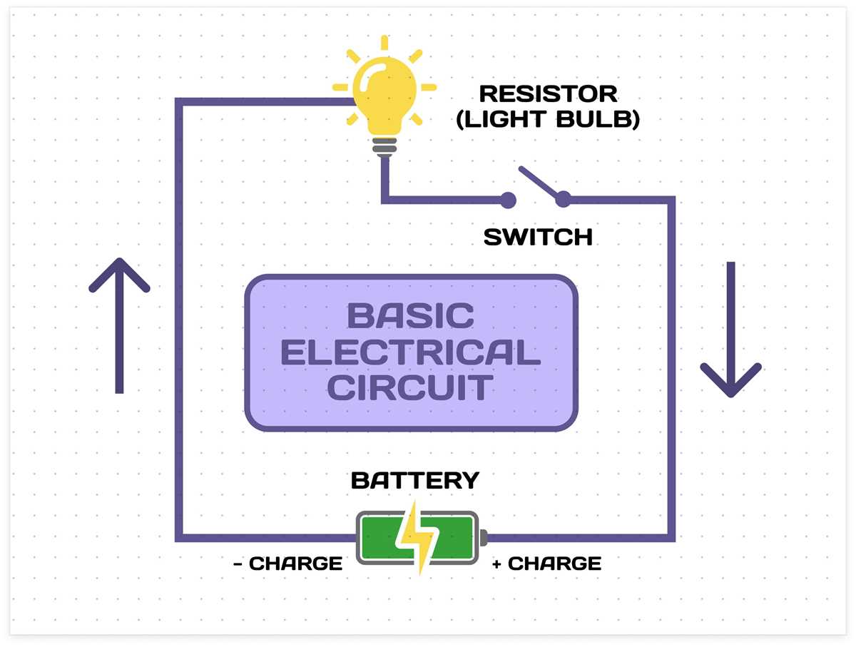
Assign a clear identifier to each component and mark terminals explicitly. Use consistent alphanumeric labels for resistors, capacitors, and modules, ensuring polarity and orientation are visible for correct assembly.
Map all connections systematically on a visual grid. Arrange components logically, maintaining straight or slightly curved lines for traces, and avoid crossing paths that could introduce interference or errors during testing.
Color code or style lines to differentiate power, ground, and signal paths. Use red for positive voltage rails, black for ground, and distinct colors for separate data lines. This prevents misrouting and makes debugging faster.
Check continuity and verify node assignments before finalizing. Trace each path from sources to loads, ensuring each junction is labeled and there are no unintentional shorts or open connections that might affect functionality.
Simulate or prototype the layout using software or breadboard testing. Validate connections under expected voltage and current conditions. Adjust component spacing, trace widths, and labels for accessibility and long-term maintenance reliability.
Choosing Components and Understanding Their Symbols
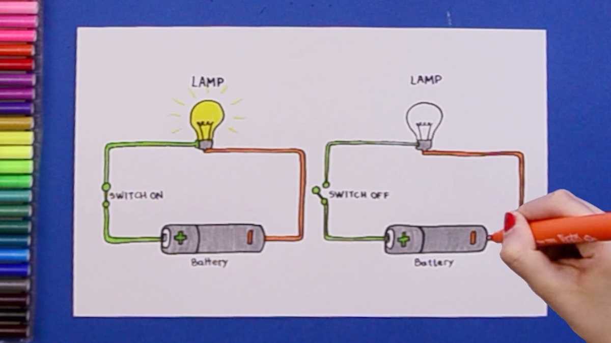
Select resistors, capacitors, and semiconductors based on their ratings. Check voltage, current, and tolerance values carefully. Using a resistor with a higher wattage than needed prevents overheating, while capacitor voltage ratings should exceed expected supply levels.
Identify components using standard schematic symbols. A resistor is represented by a zigzag or rectangular line, a capacitor by parallel lines, and diodes with a triangle pointing to a line. Proper interpretation of these symbols avoids incorrect placement or polarity errors.
Use datasheets to confirm pin assignments and electrical characteristics. For transistors and ICs, locate emitter, collector, and base or pin numbers precisely. Understanding pinout diagrams prevents damage and ensures intended functionality.
Maintain consistency when labeling components in layouts. Assign unique codes such as R1, C2, or Q3, and match them to symbols on the plan. This practice facilitates troubleshooting and provides clear guidance for assembly or modifications.