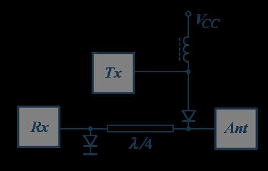
Connect each semiconductor switch with correct polarity to prevent reverse current damage. Use a stable biasing source to control signal routing accurately across the network.
Separate high-frequency paths from control lines to minimize interference. Label each connection and verify continuity before powering the assembly to ensure reliable operation.
Include current-limiting resistors in series with switching elements to prevent overload and maintain voltage stability. Confirm voltage levels with a multimeter before activating the full network.
Map signal flow visually using arrows or color codes to track input and output paths. This practice simplifies troubleshooting and future modifications while avoiding unintended feedback loops.
Pin Diode Layout Showing Component Connections and Signal Flow in Electronics
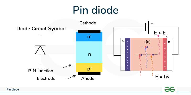
Arrange switching elements in parallel or series depending on signal requirements to reduce insertion loss. Ensure each node has clear labeling for input and output paths to prevent misconnection during assembly.
Use separate traces for control voltage lines to avoid interference with main signal paths. Maintain a minimum spacing of 2 mm between high-frequency tracks to reduce crosstalk and signal distortion.
Integrate current-limiting resistors at each control terminal. For typical 5 V logic biasing, select resistors in the range of 100–220 Ω to protect switches and maintain stable operation across temperature variations.
Mark RF or high-speed lines with color codes or labels to track signal direction. This helps technicians verify connectivity quickly and reduces the chance of routing errors in complex assemblies.
Place decoupling capacitors near biasing points to suppress voltage fluctuations. Recommended values are 10–100 nF for typical low-power switching networks, positioned as close as possible to terminals.
Verify all solder joints visually and with continuity testing before powering the network. Even small cold joints can cause signal attenuation or intermittent operation in sensitive electronic paths.
Document control and signal paths in a simple table listing each element, terminal, and expected voltage. This provides a quick reference for maintenance and troubleshooting.
Test signal flow progressively by applying low-level inputs and measuring outputs at each stage. Adjust bias voltages as needed to confirm correct activation of each switching element without overloading any branch.
Identifying Pin Diode Connections and Polarities
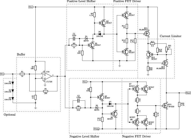
Check polarity markings on each switch element before installation. Most components include a band or symbol indicating cathode and anode terminals, which must align with the biasing voltage to function correctly.
Use a multimeter in forward voltage mode to confirm terminal orientation. A correctly connected element shows a small voltage drop around 0.7 V, whereas reversed leads display open-circuit behavior.
Label control and signal terminals clearly on the assembly board. Maintaining a consistent labeling scheme prevents accidental swaps and ensures that switching elements respond predictably during operation.
Follow the recommended biasing polarity provided in manufacturer specifications. For high-speed switching, even slight deviations can increase insertion loss or create unwanted reflections in RF paths.
Observe trace routing near terminals to verify that high-current and low-current paths do not intersect. Misrouting can lead to voltage drops and inconsistent switching behavior under load conditions.
Confirm connectivity with continuity tests before soldering or final assembly. This step ensures that each element’s anode and cathode link correctly to the intended nodes and prevents polarity mistakes from affecting downstream stages.
Keep spare test points near each terminal to allow voltage monitoring during operation. Measuring these points can quickly reveal reversed connections or misapplied bias without dismantling the network.
Document each element’s orientation and control connections in a simple table or schematic for maintenance. This reference reduces errors when replacing components or making adjustments to the switching assembly later.